
Our own production facilities
See our Shenzhen production lines, equipment and inspection processes. You work directly with JETFGO, the manufacturer.
View factory process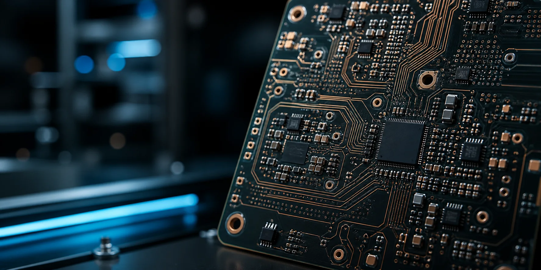
JETFGO owns and operates PCB factories in Shenzhen, China. We manufacture printed circuit boards and provide PCB assembly, with our own engineering, production and quality teams serving distributors, trading companies and OEM/EMS buyers directly.
Give your sales and procurement teams a clearer path from customer requirement to manufacturable order, supported by visible factory, process, capability and certification records.
See our Shenzhen production lines, equipment and inspection processes. You work directly with JETFGO, the manufacturer.
View factory processConfirm stackup, materials, testing, quantity and target date before the build is released.
Check capability limitsUse published ISO, IATF, UL and quality documents for supplier review and customer approval.
Review certificatesCarry approved engineering inputs into repeat orders with revision and inspection requirements kept visible.
Open supplier documentsChoose the end environment, construction and primary constraint. The selector recommends relevant technical pages for your RFQ; final feasibility is confirmed during DFM review.
Process discipline for vehicle control, power and sensing electronics.
3 / Solutions02Industrial ControlRobust multilayer and PCBA solutions for long-life industrial systems.
3 / Solutions03Communications & AI InfrastructureHigh-speed, HDI and RF boards for data-intensive platforms.
3 / Solutions04Medical ElectronicsCompact, reliable interconnects for diagnostic and treatment equipment.
3 / Solutions05Aerospace & DefenseHigh-reliability RF, rigid-flex and lifecycle support for mission-sensitive electronics.
3 / Solutions06Renewable Energy & PowerThermal and current-carrying PCB paths for conversion, storage and power control.
3 / Solutions07Robotics & AutomationCompact interconnect, motion-ready flex and control electronics for automated equipment.
3 / Solutions08Consumer & Smart HardwareDensity, miniaturization and integrated assembly for connected devices and smart products.
3 / SolutionsGive distributors and sourcing teams one technical route across conventional, HDI, RF, flex, rigid-flex and PCBA requirements—from DFM review to documented inspection.
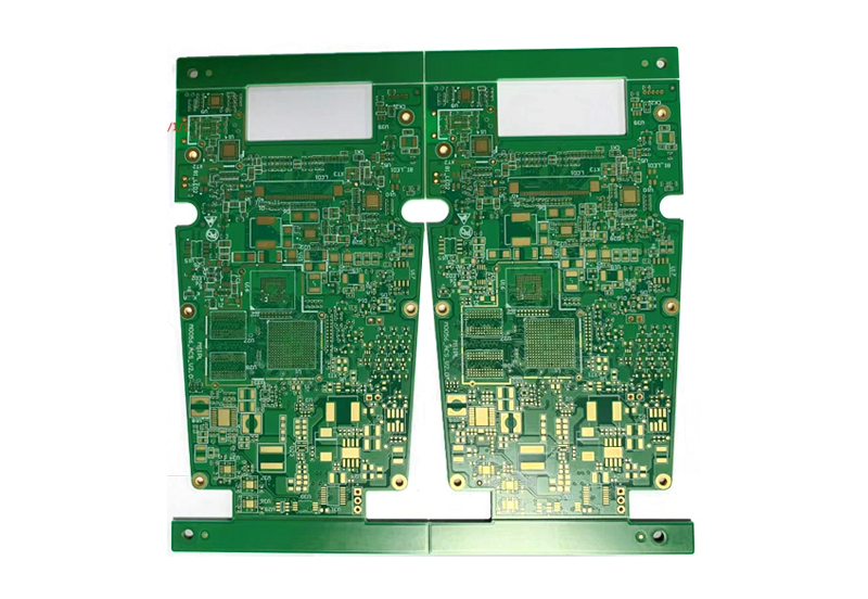
Reliable single- and multilayer boards for industrial, communications, computer and medical electronics.
View details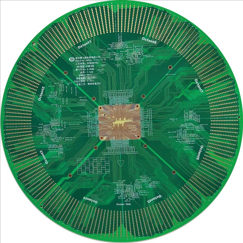
Microvias, sequential lamination and fine-line routing for compact, high-density electronics.
View details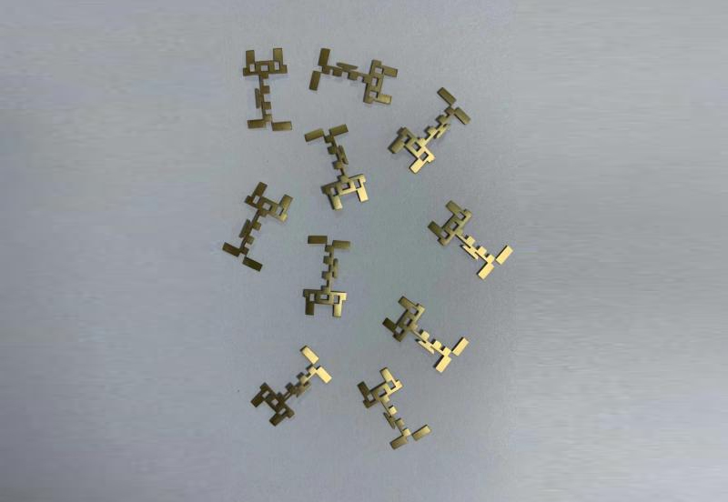
Low-loss laminates, controlled dielectric behavior and repeatable RF performance.
View details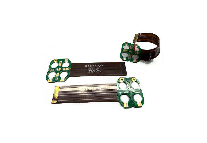
Integrated rigid and flexible circuits for compact assemblies and dynamic interconnects.
View details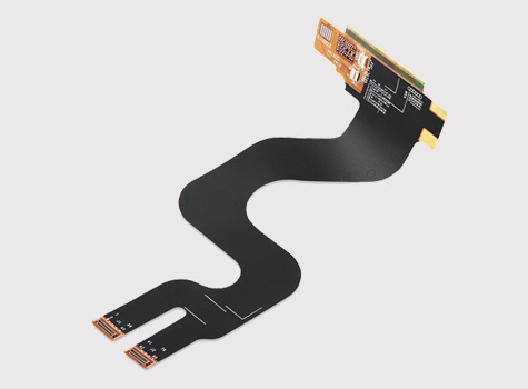
Fine-feature flex circuits with sheet or roll-to-roll production and assembly-test support.
View details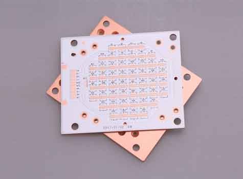
Aluminum, copper and specialty metal-base constructions for demanding thermal and power designs.
View details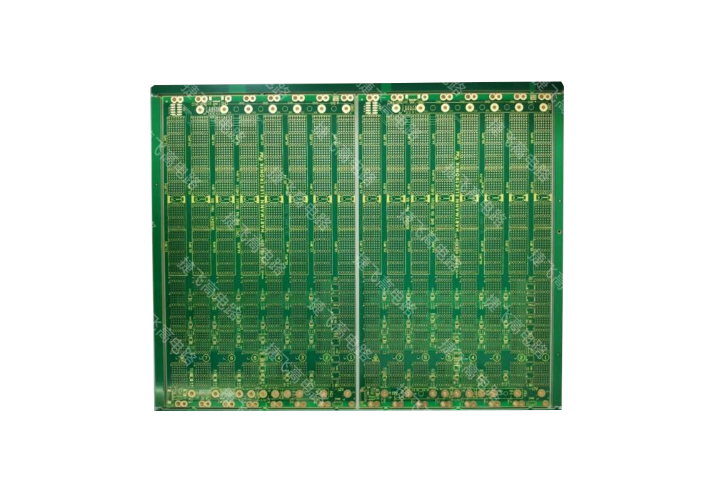
Complex multilayer structures for reliable prototypes and scalable medium-volume production.
View details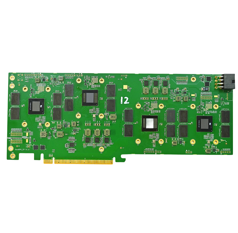
One-stop SMT, through-hole, testing, conformal coating and box-build coordination.
View details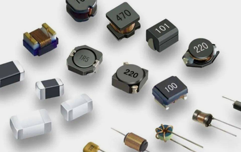
BOM-based component sourcing, traceability review and supply coordination connected to PCBA delivery.
View detailsEach page turns one common customer need into a clear manufacturing route, published capability limits and an RFQ file checklist your team can reuse.
A DFM-led prototype path for urgent design verification and controlled transition into repeat production.
Open solutionSI-04LA practical stackup path for interfaces that need predictable single-ended or differential impedance.
Open solutionHS-06LStackup, reference-plane and back-drill review for data-intensive boards where signal integrity drives manufacturability.
Open solutionHDI-1N1A density-led build path for compact layouts, fine-pitch BGAs and laser-drilled interconnects.
Open solutionRF-4350Material-control and impedance-review path for microwave, antenna and RF signal chains.
Open solutionHYB-RFA mixed-material route that places RF performance only where it is needed while retaining a practical multilayer structure.
Open solutionFLEX-MLPolyimide construction for compact, moving or space-constrained interconnects with defined bend and routing needs.
Open solutionRFX-06LIntegrated rigid and flexible regions for compact assemblies that need fewer connectors and controlled transitions.
Open solutionMCPCB-ALA metal-core path for boards where thermal transfer and mechanical construction drive the design.
Open solutionHCP-06OZ+A current-carrying and thermal path for power conversion, drives and high-load industrial electronics.
Open solutionAUTO-IATFA documentation- and traceability-led path for vehicle control, sensing and power electronics.
Open solutionPCBA-BOXOne accountable workflow connecting BOM review, sourcing, PCB fabrication, SMT, THT, testing and final assembly.
Open solutionLIFE-CYCLEA controlled path for obsolete components, missing fabrication data, material substitutions and repeat builds of long-life equipment.
Open solutionPublished limits are drawn from JETFGO’s current capability chart. Final feasibility depends on the complete data package and engineering review.
Use published process limits, equipment and inspection controls to qualify the order, explain constraints and prepare a more complete customer quotation.
Explore capabilitiesBuy directly from the manufacturer. Our own factory teams review DFM, plan production and inspect your boards, with equipment and process records available for supplier qualification.
Engineering review
Material & stackup
Precision fabrication
Inspection & delivery
Our own factories manufacture prototypes and low-to-medium volume PCB orders, with our engineering and quality teams responsible for material review, inspection and repeat-order consistency.
Process discipline for vehicle control, power and sensing electronics.
View detailsRobust multilayer and PCBA solutions for long-life industrial systems.
View detailsHigh-speed, HDI and RF boards for data-intensive platforms.
View detailsCompact, reliable interconnects for diagnostic and treatment equipment.
View detailsHigh-reliability RF, rigid-flex and lifecycle support for mission-sensitive electronics.
View detailsThermal and current-carrying PCB paths for conversion, storage and power control.
View detailsCompact interconnect, motion-ready flex and control electronics for automated equipment.
View detailsDensity, miniaturization and integrated assembly for connected devices and smart products.
View detailsPractical, reusable guidance for preparing RFQs, checking manufacturability and qualifying a PCB supply route.
The data, stackup and fabrication decisions that prevent avoidable delays.
View detailsHow build structure, via geometry and materials shape HDI manufacturability.
View detailsA practical framework for material choice, geometry, coupons and tolerances.
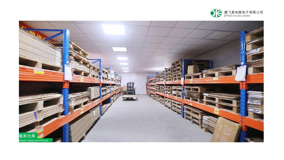
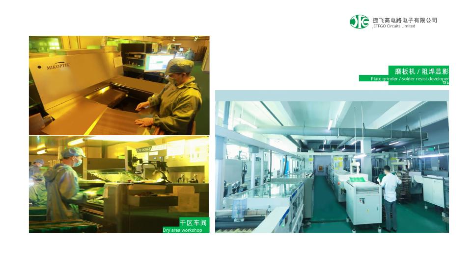
View detailsJETFGO owns and operates these PCB factories. Explore our production equipment, manufacturing processes and inspection systems before sourcing directly from us.
Send the Gerber or ODB++, stackup, material, quantity, target date and test requirements. Our team will review feasibility and return a technical quotation for the order you manage.