
Engineering review
Our own factories manufacture prototypes and low-to-medium volume PCB orders, with our engineering and quality teams responsible for material review, inspection and repeat-order consistency.
Embedded copper inlays create a direct thermal path for high-power and high-heat-density assemblies. Our own factories manufacture prototypes and low-to-medium volume PCB orders, with our engineering and quality teams responsible for material review, inspection and repeat-order consistency.
Get a factory-direct quote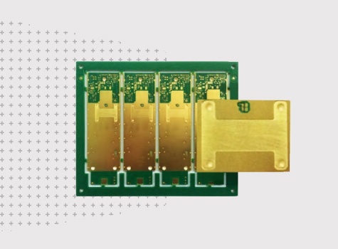 PRODUCT & PROCESS DETAIL
Buy directly from the manufacturer. Our own factory teams review DFM, plan production and inspect your boards, with equipment and process records available for supplier qualification.
Buy directly from the manufacturer. Our own factory teams review DFM, plan production and inspect your boards, with equipment and process records available for supplier qualification.
Our own factories manufacture prototypes and low-to-medium volume PCB orders, with our engineering and quality teams responsible for material review, inspection and repeat-order consistency.
A transparent capability framework for multilayer, HDI, high-speed, RF and rigid-flex builds.
Embedded copper inlays create a direct thermal path for high-power and high-heat-density assemblies.
Use published process limits, equipment and inspection controls to qualify the order, explain constraints and prepare a more complete customer quotation.
Embedded copper inlays create a direct thermal path for high-power and high-heat-density assemblies.
Embedded copper inlays create a direct thermal path for high-power and high-heat-density assemblies.
Gerber or ODB++, fabrication drawing, stackup, quantity, material, surface finish and controlled requirements. Add the BOM and pick-and-place files for PCBA.
Yes. The factory is organized for quick prototypes and scalable low-to-medium volume production, keeping the engineering record connected between builds.
The control plan may include incoming material checks, AOI, electrical test, impedance verification, dimensional inspection and final QA according to the build.
Send the Gerber or ODB++, stackup, material, quantity, target date and test requirements. Our team will review feasibility and return a technical quotation for the order you manage.