
PCB製品・用途
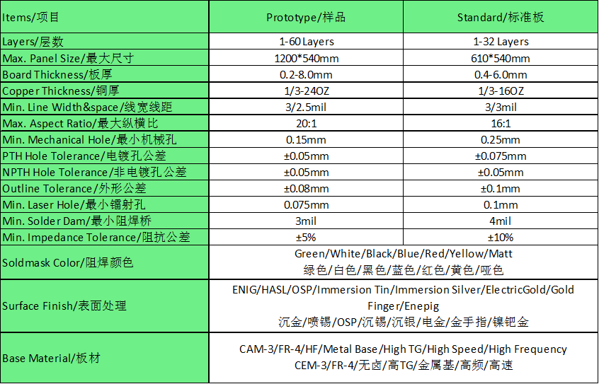
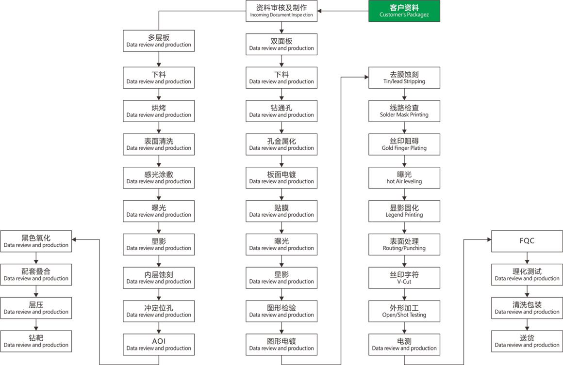
PCBA技術・設備
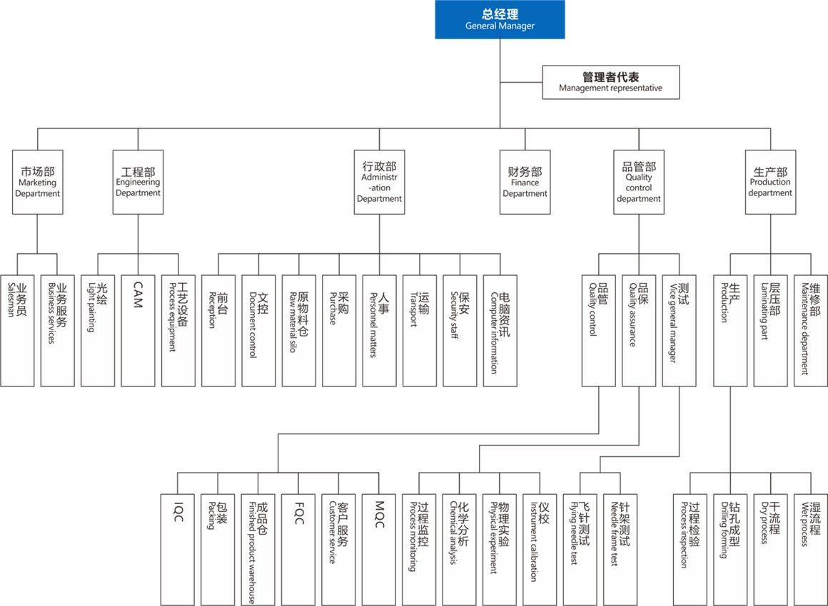
05品質・管理
製品・用途
58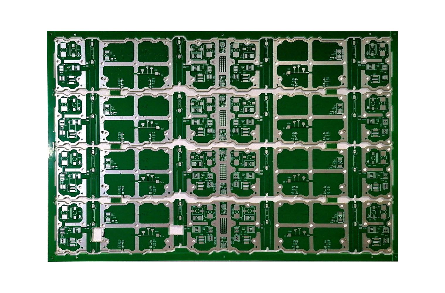
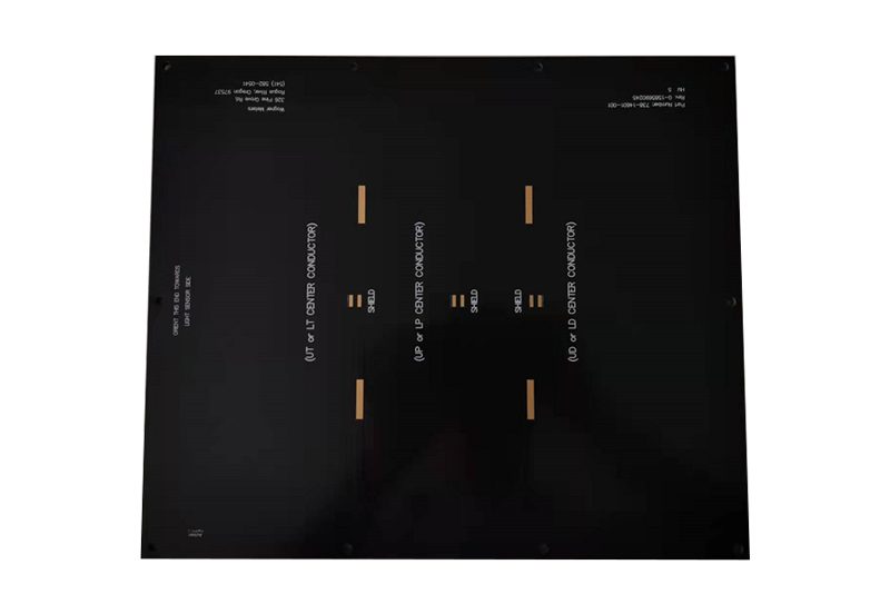
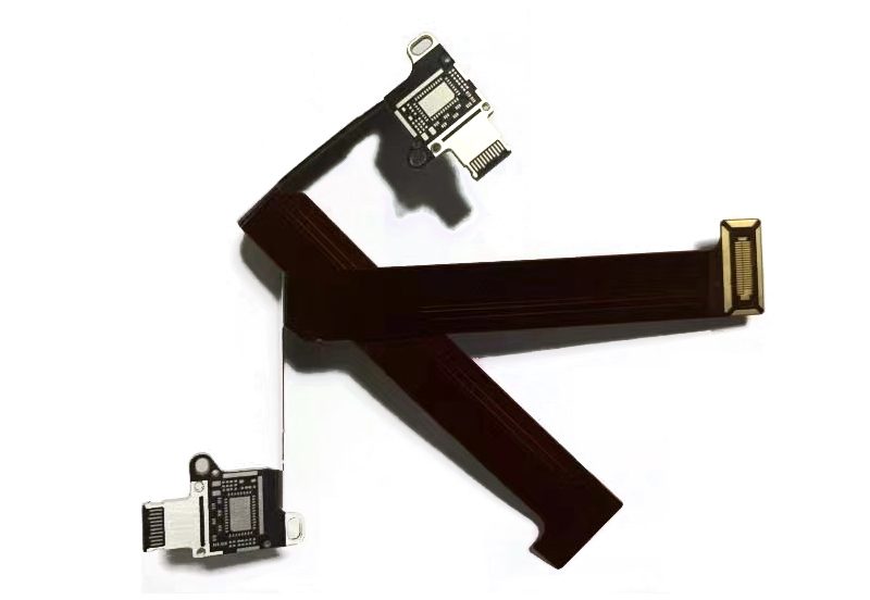
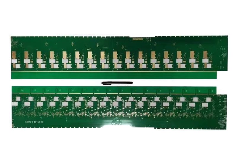
Antenna Board
Layers: 6 Material: FR-4 Surface Finish: Immersion Silver Board Thickness: 2.2mm Line Width & Space: 7.5 / 4mil Special Technology: Impedance
詳細を見る
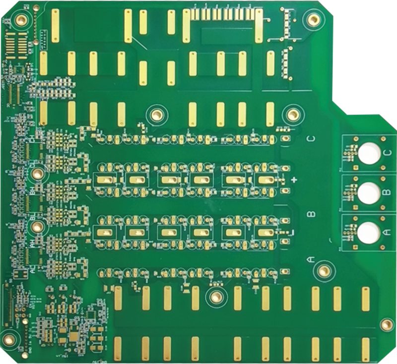
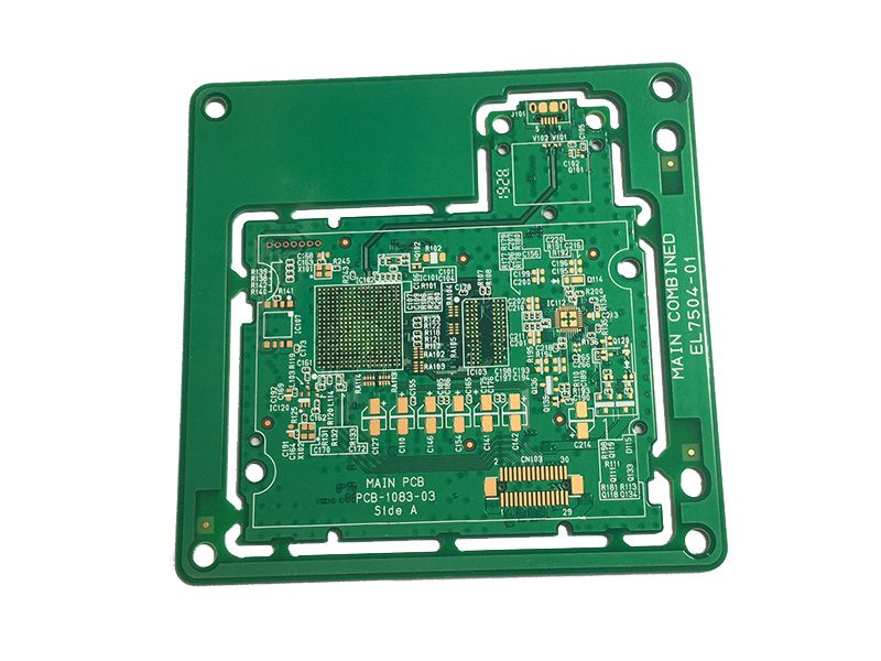
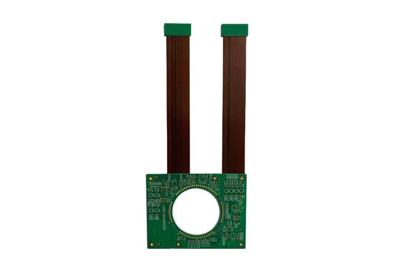
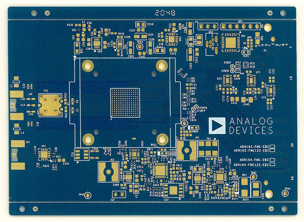
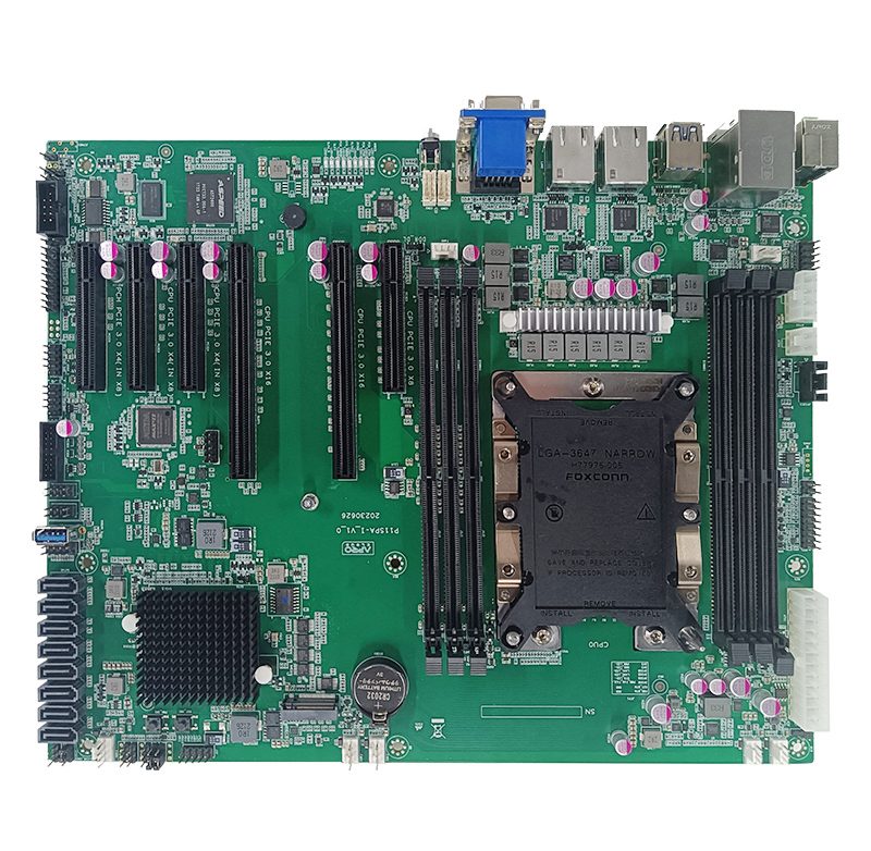
Computer Board
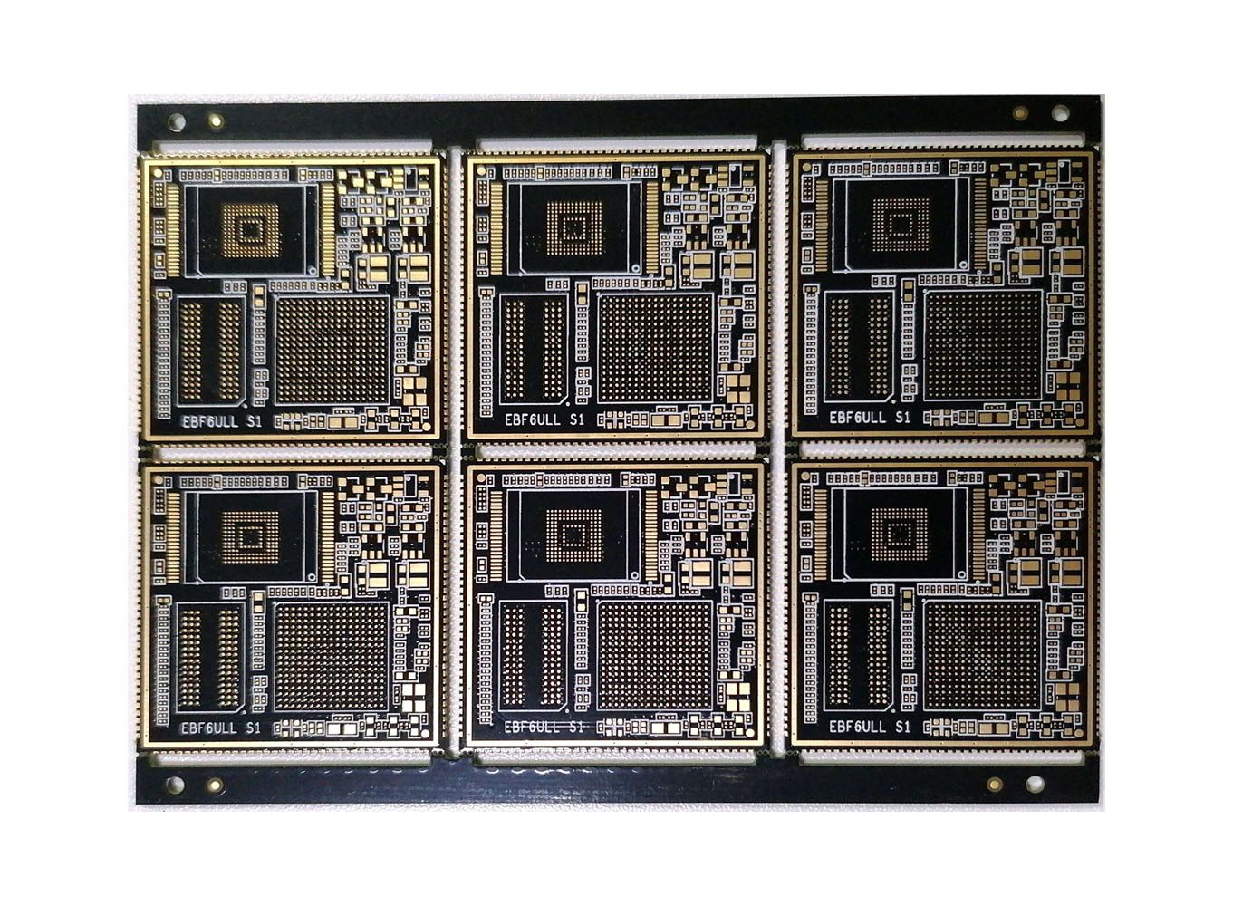
Layers: 8 Material: FR-4 Surface Finish: ENIG Board Thickness: 1.1mm Line Width & Space: 4/2.5mil Special Technology: Half Hole
詳細を見る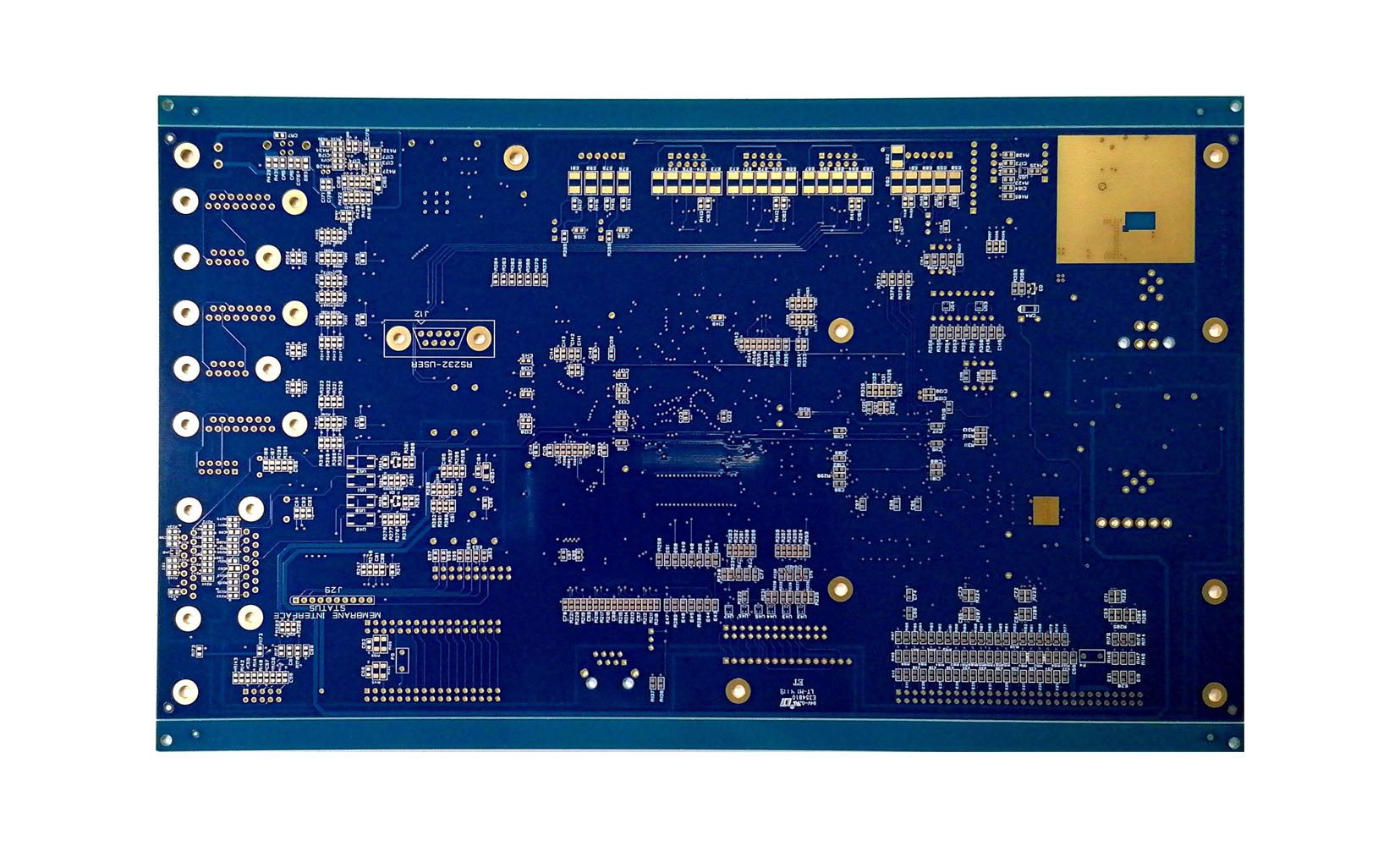
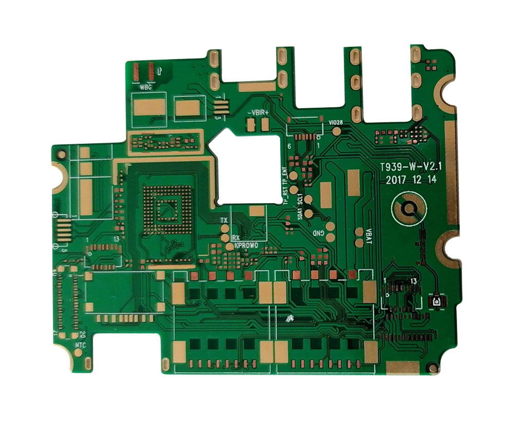
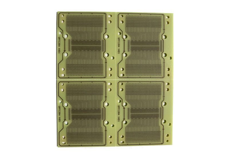
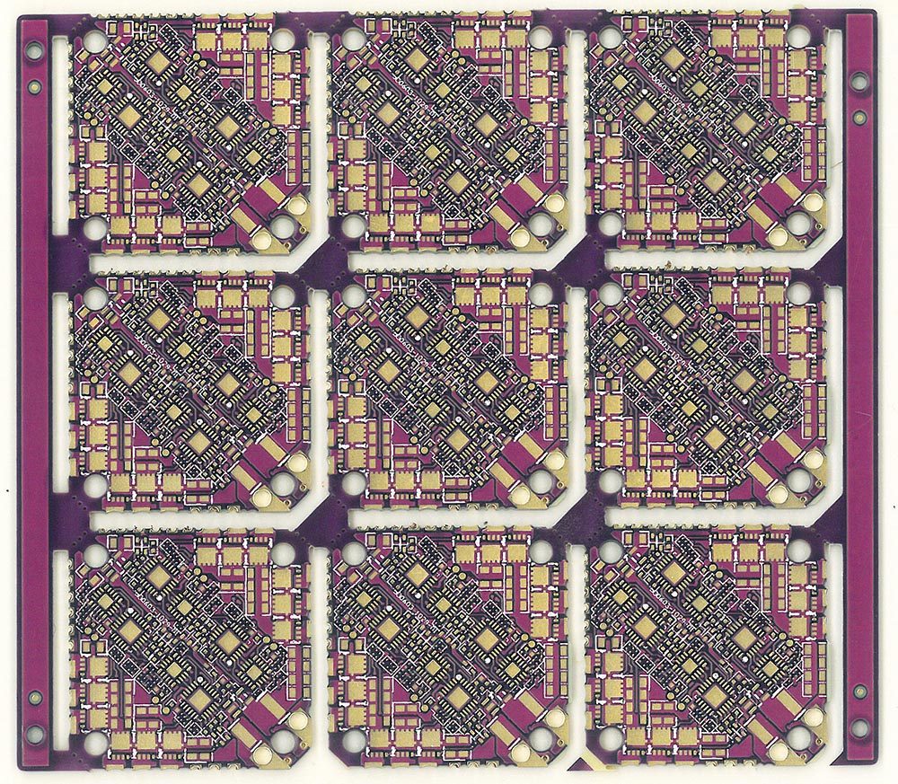
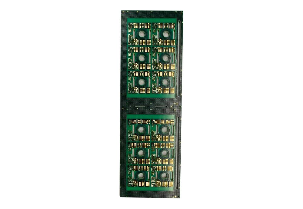
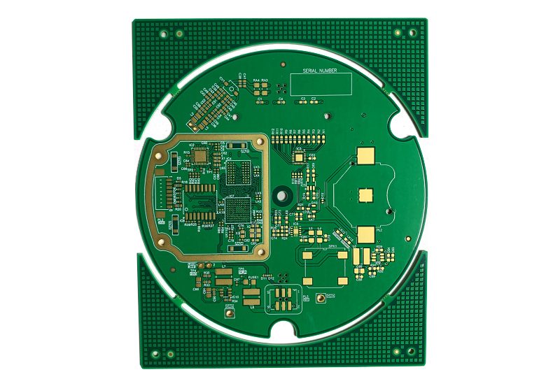
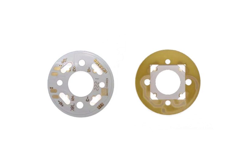
High Frequency Board
Layers: 2 Material: Rogers4003 Surface Finish: ENIG Board Thickness: 1.6mm Minimum Hole: 0.2mm
詳細を見る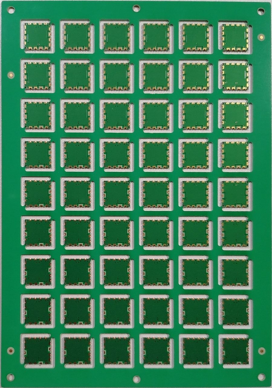
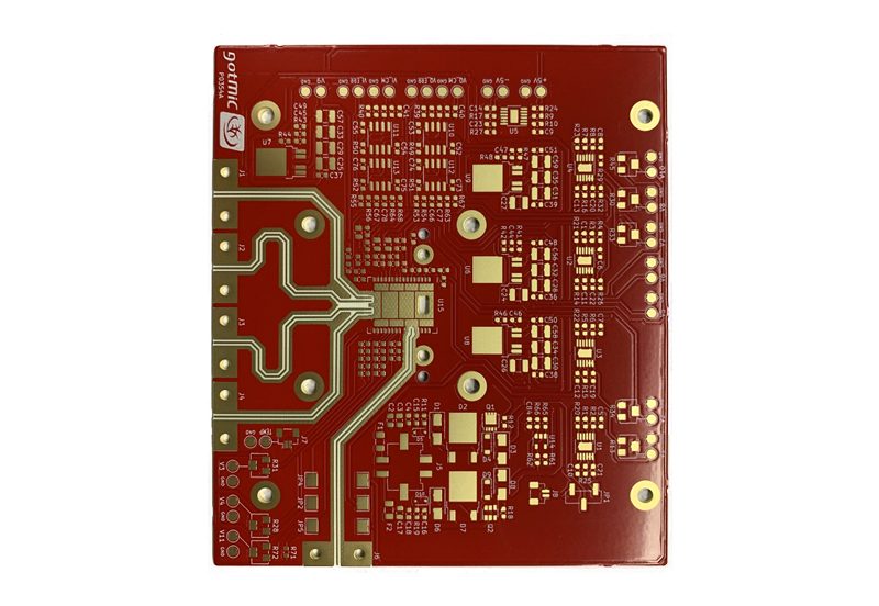
High Frequency Board
Layers: 2 Material: Rogers4350 Surface Finish: ENIG Board Thickness: 1.6mm Minimum Hole: 0.2mm Line Width & Space: 3.5 / 3.5mil Special Technology: High Frequency, Half Hole
詳細を見る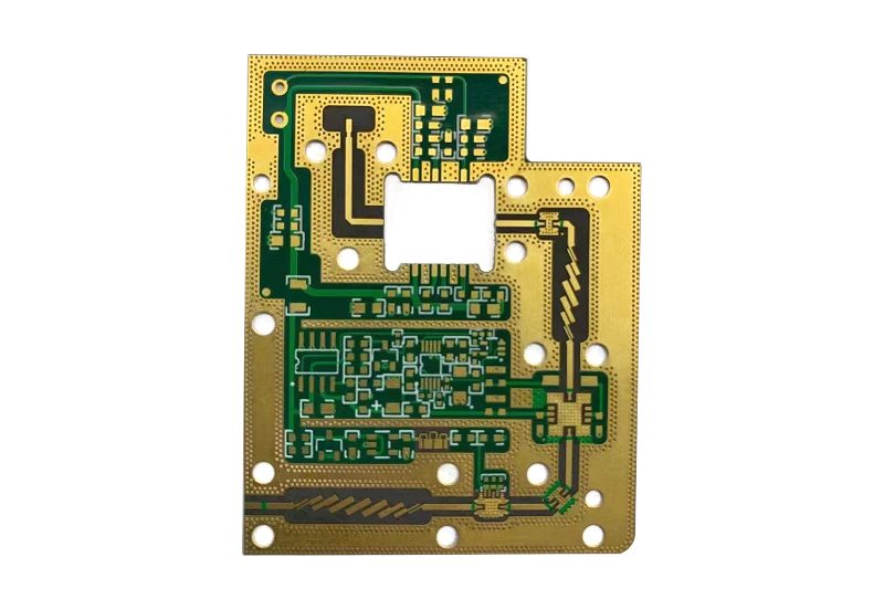
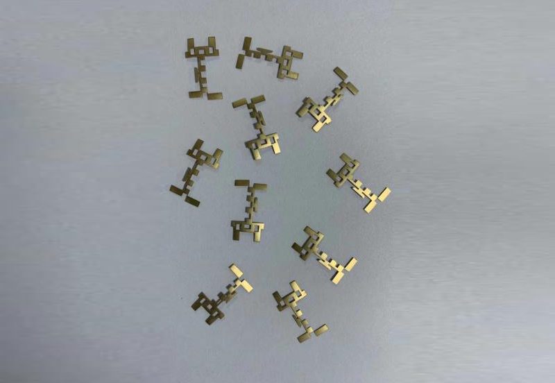
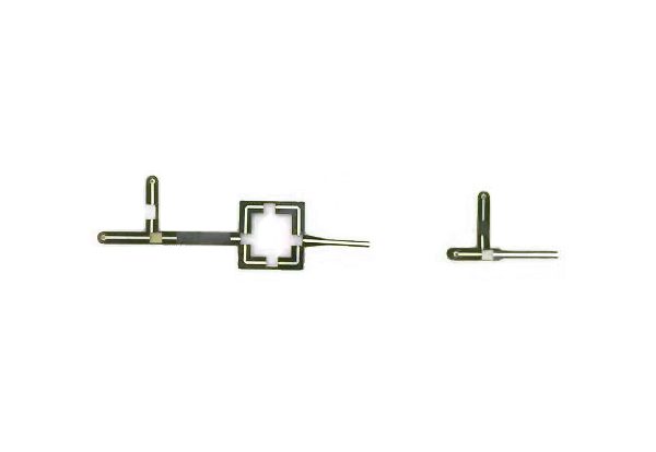
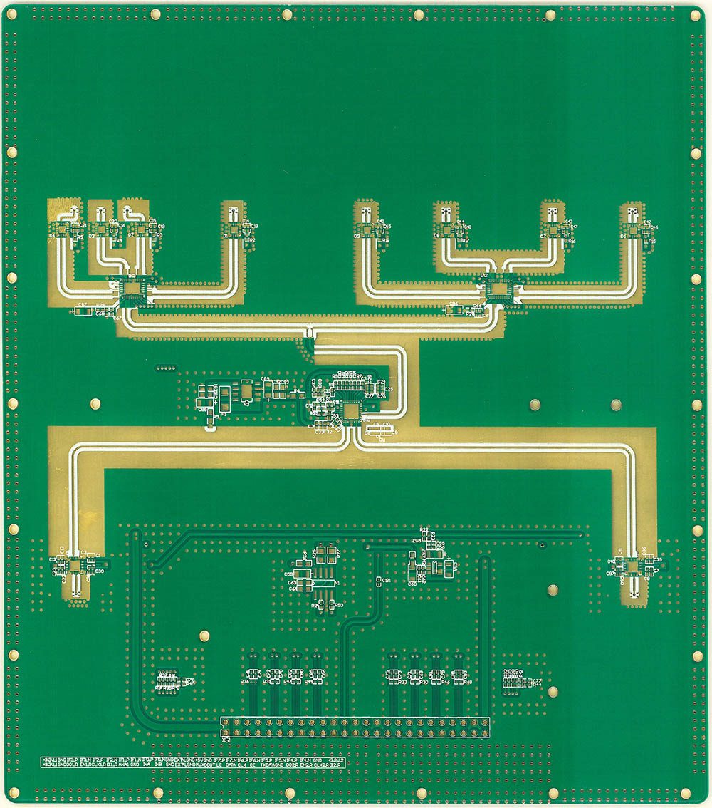
High Frequency Board
Layers: 6 Material: FR-4 Rrogers4350 Surface Finish: ENIG Sheet thickness: 1.6mm Minimum Hole:0.3mm Special Technology: High Frequency, 3 Step HDI
詳細を見る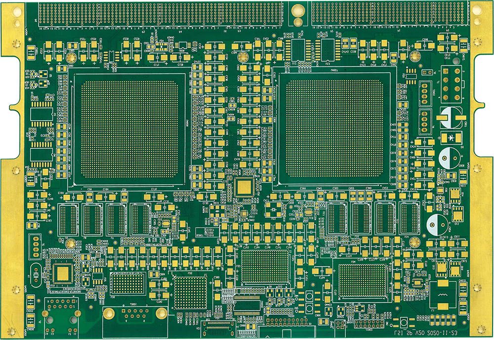
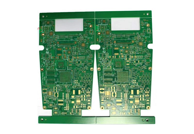
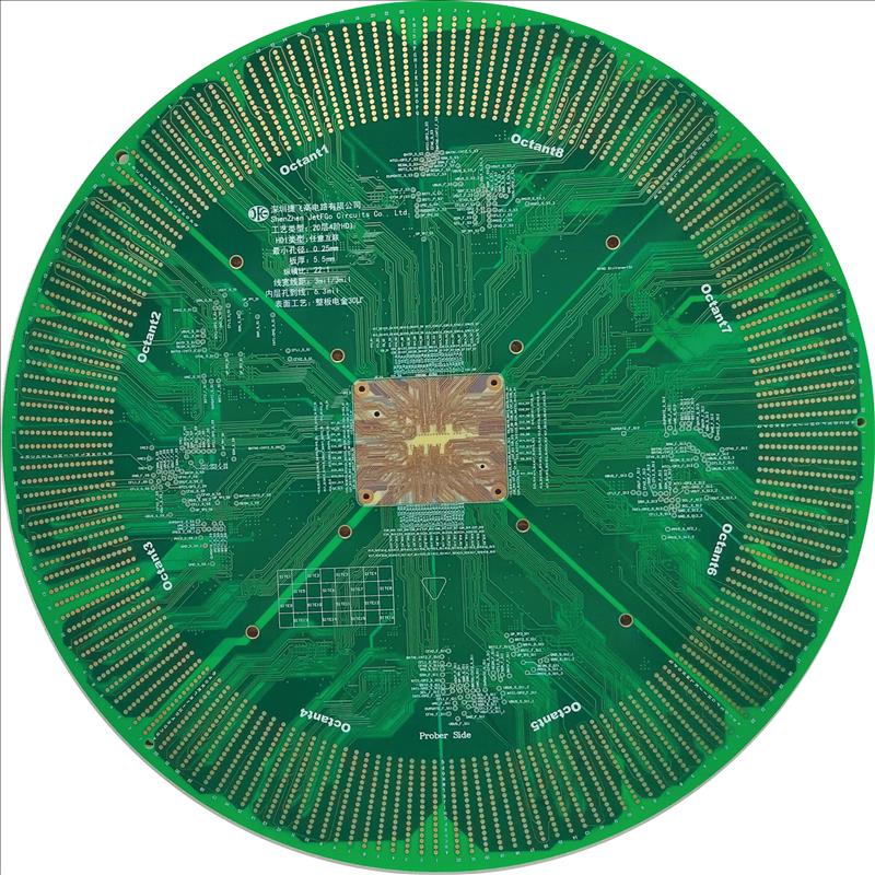
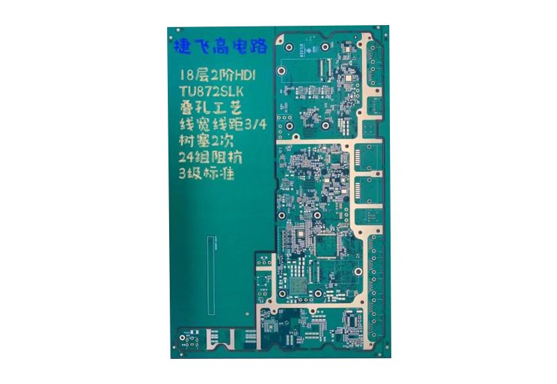
High Speed Board
Layers: 24 Material: FR-4 Panasonic M6 Surface Finish:ENIG Board Thickness: 3mm Minimum Hole: 0.25mm Line Width Space: 3.5 / 3.5mil Special Technology: Via in PAD, Back drilling, Depth milling, Impedance
詳細を見る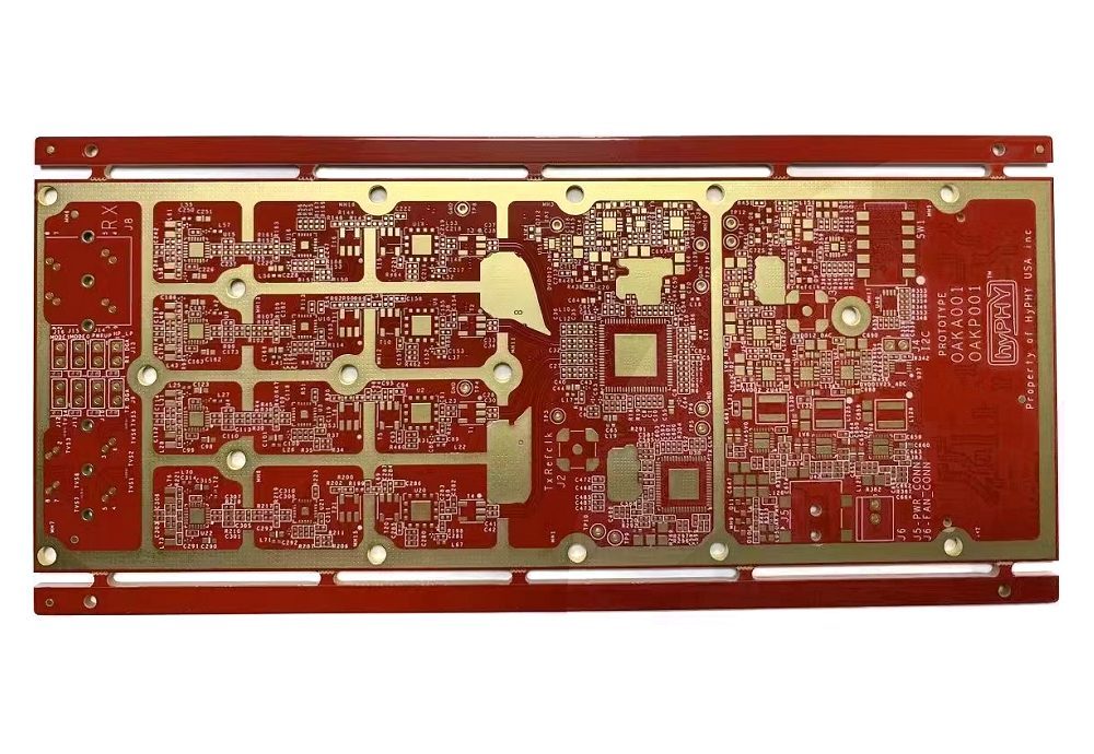
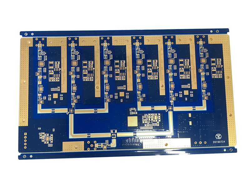
Hybrid Board
Layers: 4 Material: Rogers 4350+FR-4 Surface Finish: ENIG Board Thickness: 1.2mm Minimum Hole: 0.2mm Special Technology: Hybrid
詳細を見る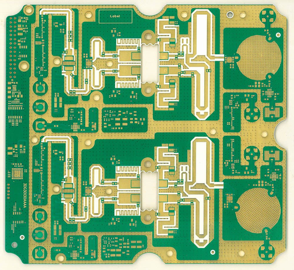
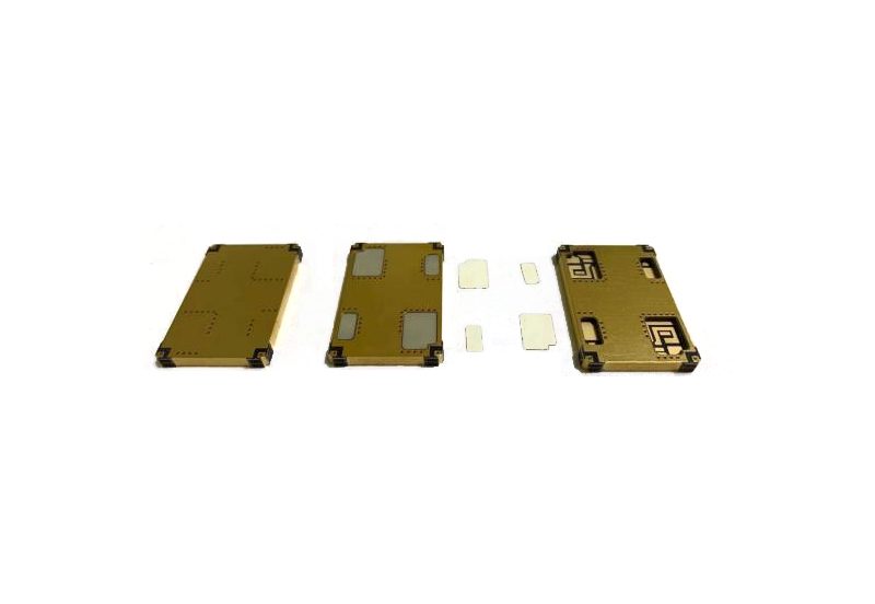
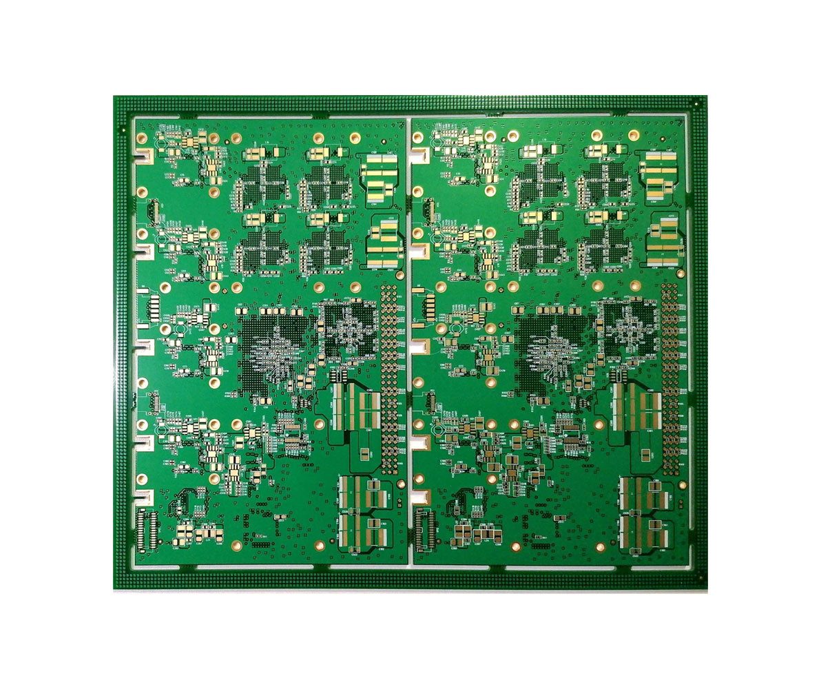
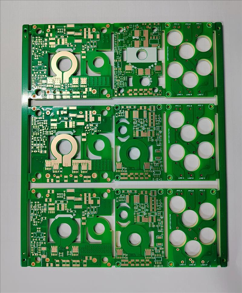
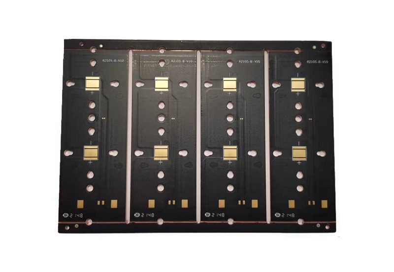
Industrial Board
Layers: 14 Material: FR-4 Surface Finish: ENIG Board Thickness: 2.0mm Line Width Space: 4.3 / 3.5mil Special Technology: Impedance
詳細を見る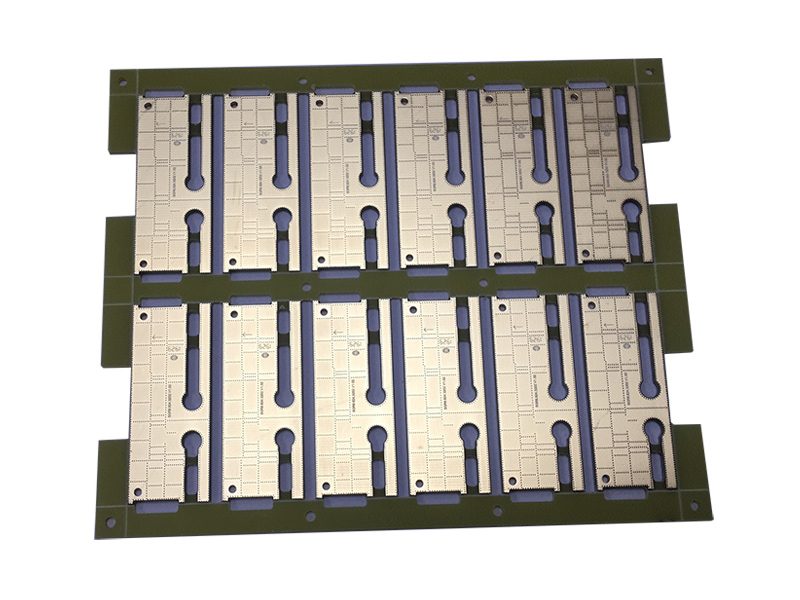
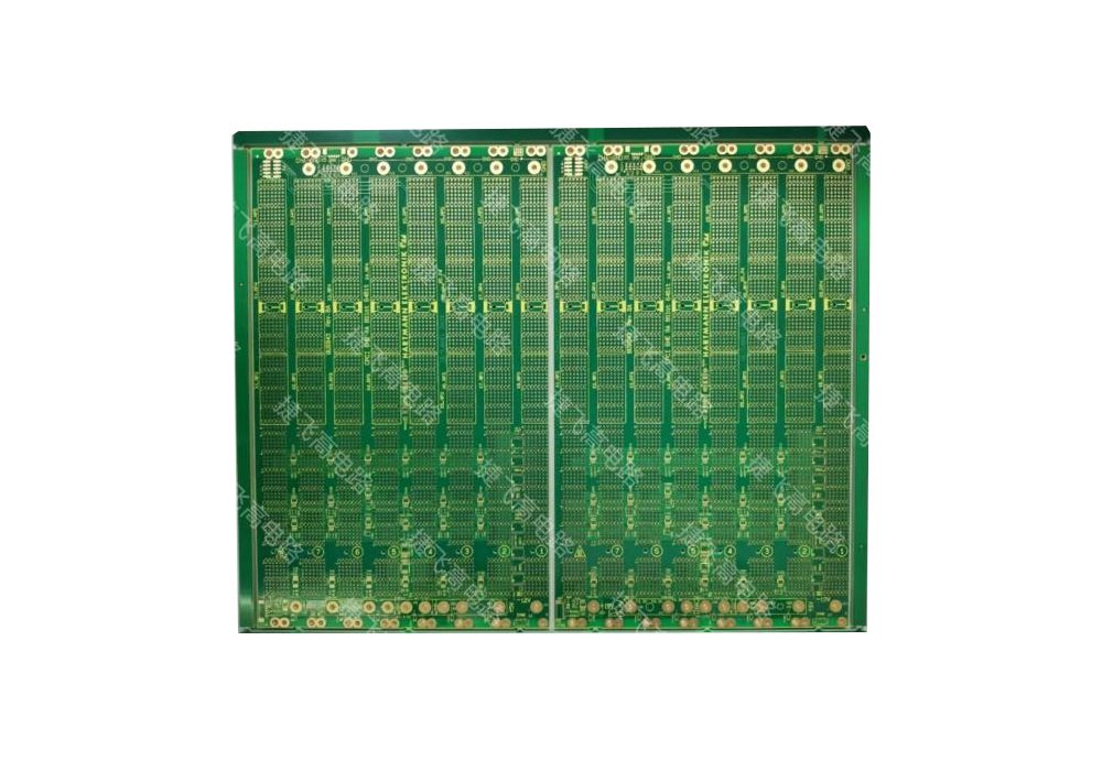
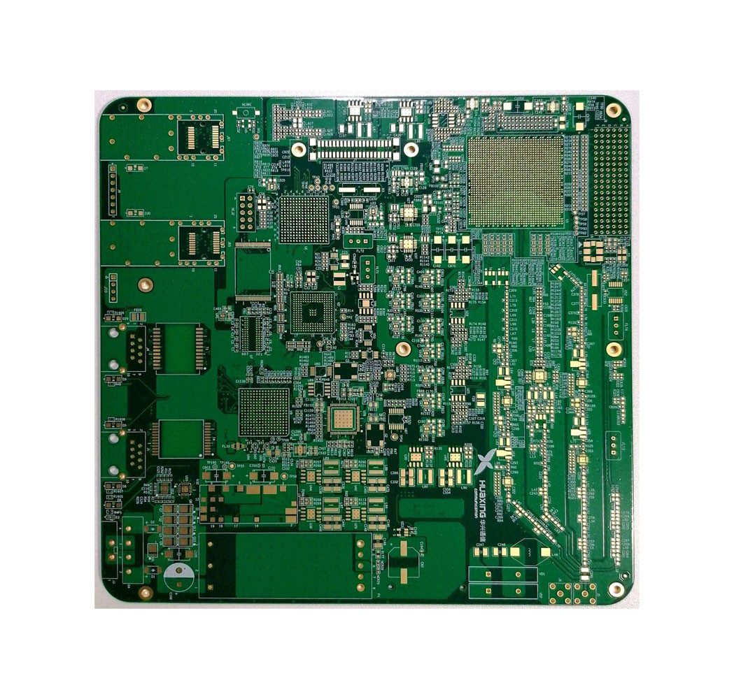
Medical Board
Layers: 10 Material: FR-4 / High Tg Surface Finish: ENIG Board Thickness: 2.0mm Line Width & Space: 5.4 / 3.5mil Special Technology: Impedance
詳細を見る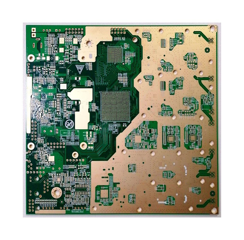
技術・設備
07

品質・管理
04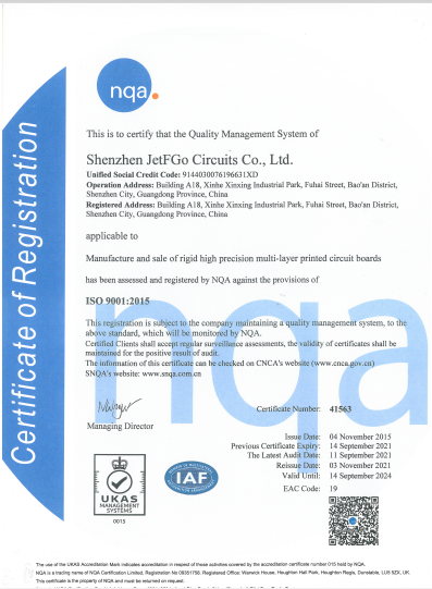
企業情報
32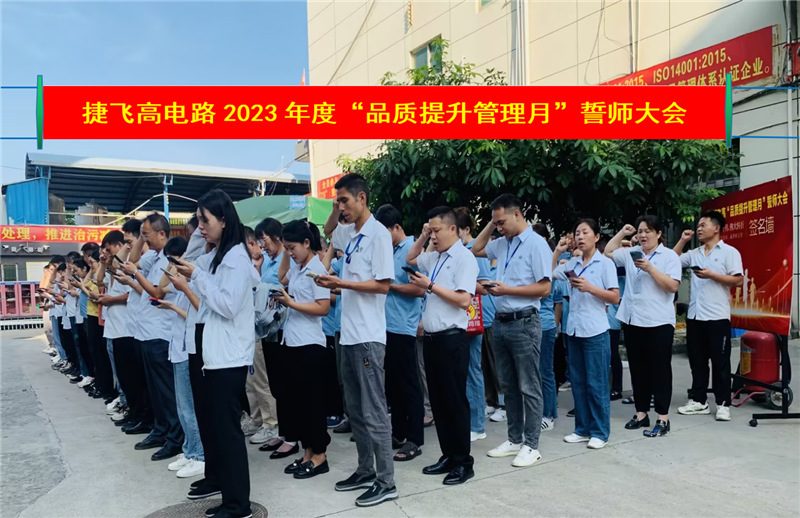
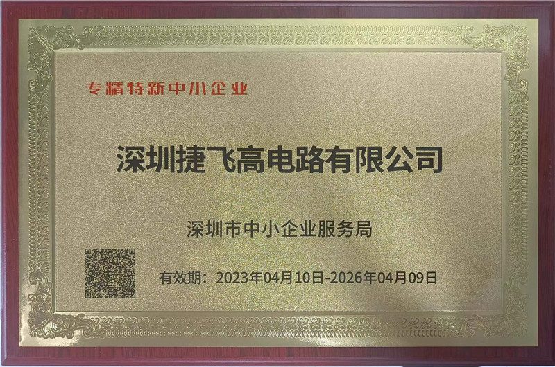
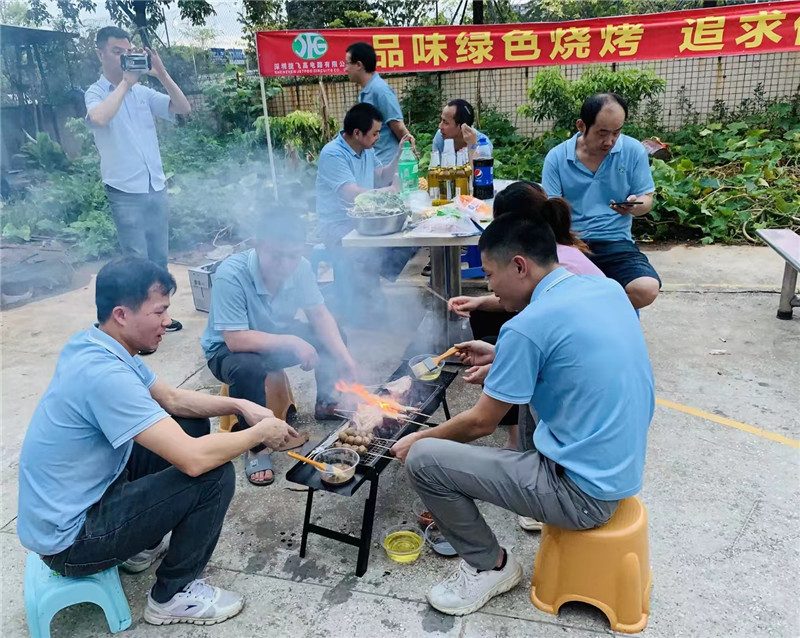



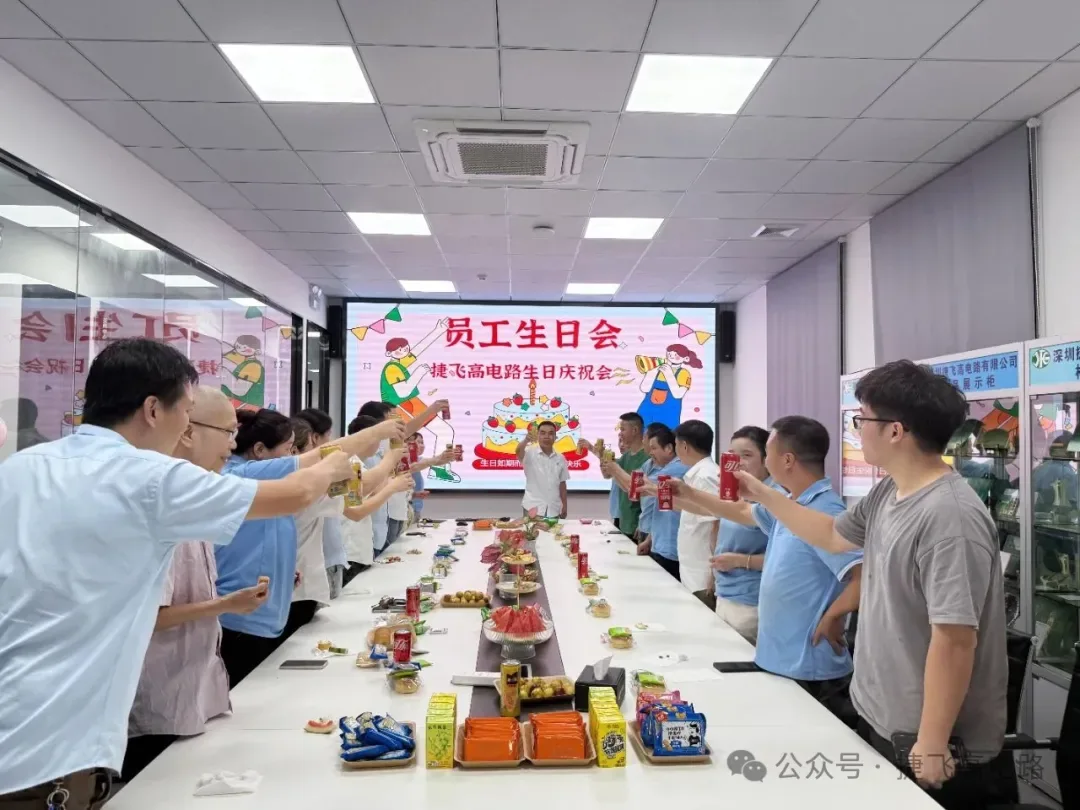
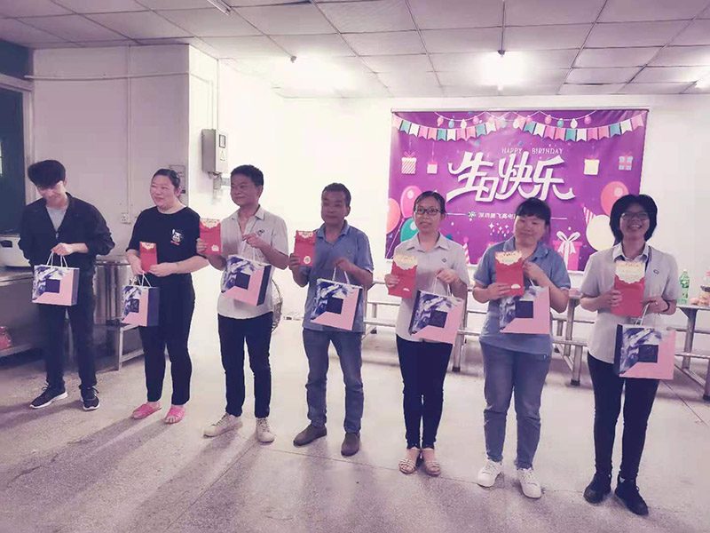




会社・文化
08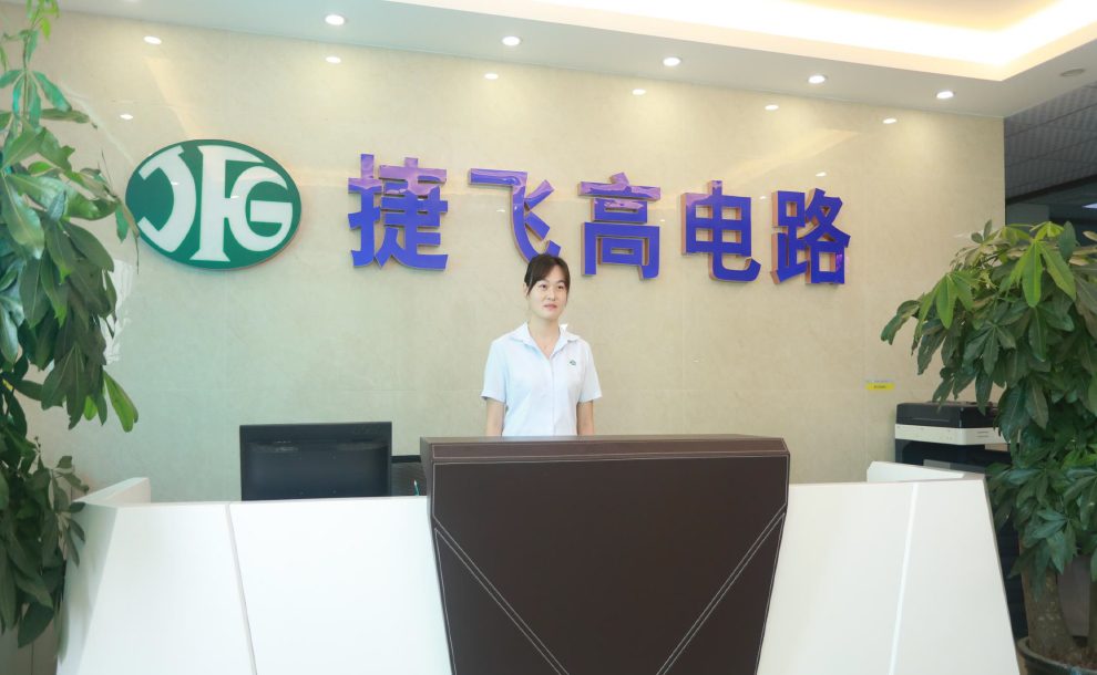
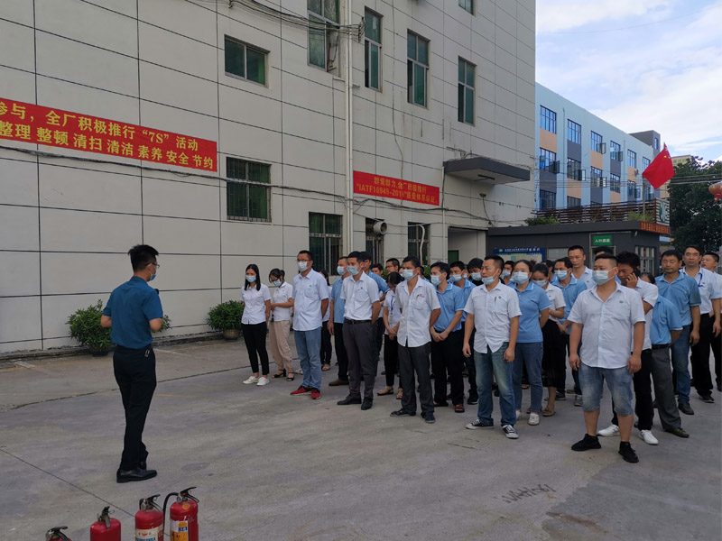
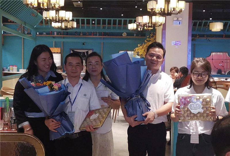
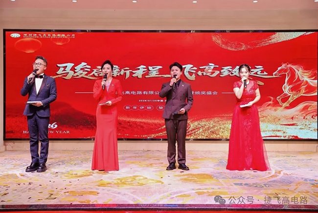
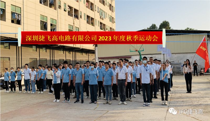
Company Culture
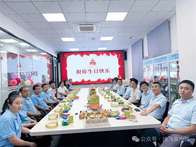
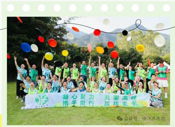
Vision Building Jiffy High Circuits into a brand enterprise in the high-end printed circuit board industry at home and abroad
詳細を見る
Company Profile
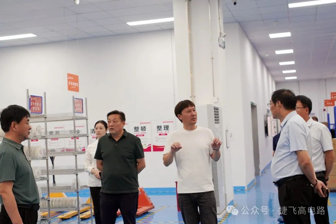
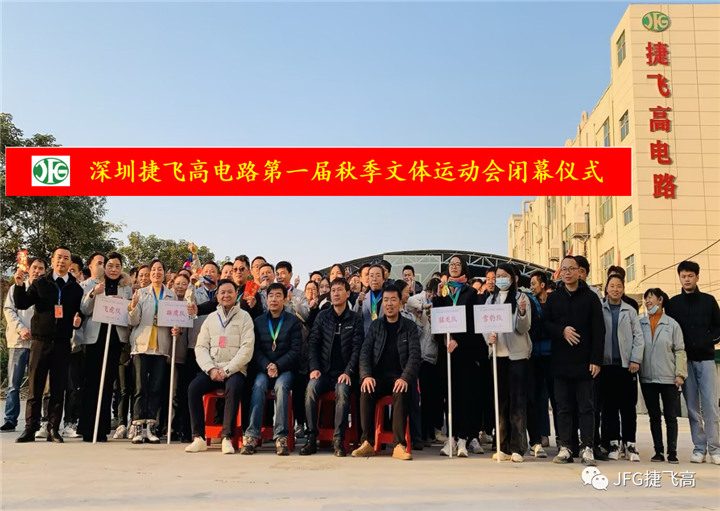
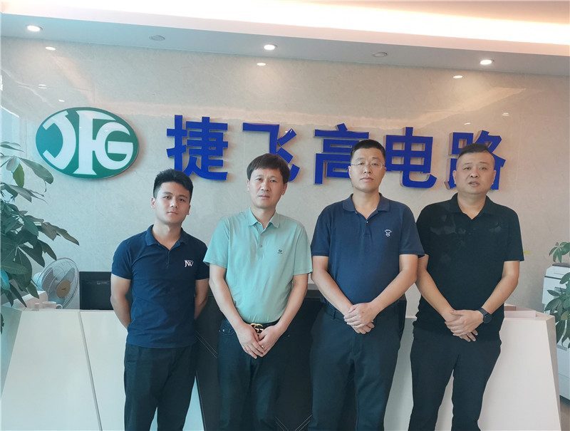
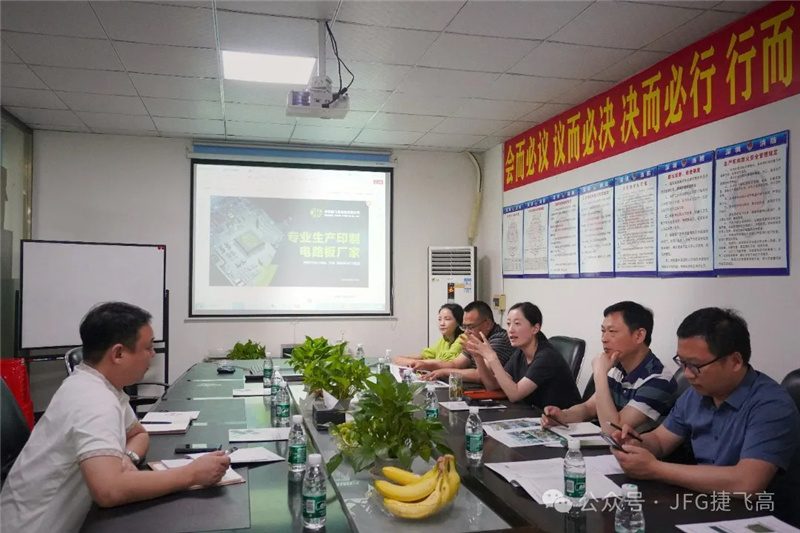
Shenzhen JETFGO Circuits Co Ltd. is a manufacturer whom specializing in the production of printed circuit boards in Shenzhen city. The company was established in 2004, and the factory is located in Fuhai Street, Bao'an D
詳細を見るJob Offers
CAM Senior Engineer 2 Shenzhen 2023-10-10 Requirements: 1. Male or female, aged 22-36, with a full-time undergraduate degree or above; 2. Must have at least 2 years of practical work experience in the same PCB position;
詳細を見る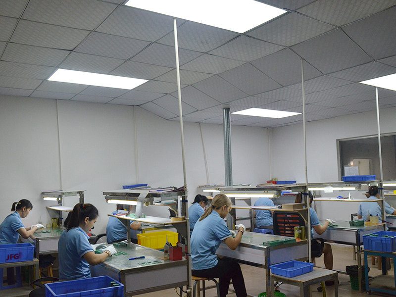
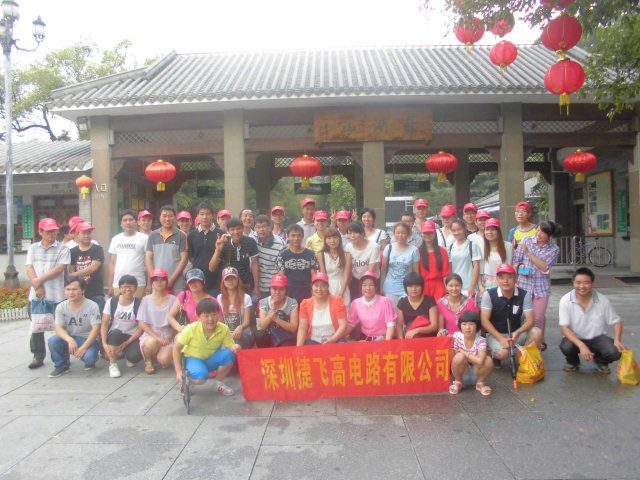
Shenzhen JETFGO Circuits Co.,Ltd.
Shenzhen JETFGO Circuits Co.,Ltd is a professional Printed Circuit Boards manufacturer in China. It was established in 1999, the factory was located at Fuyong Town, Bao’an District, Shenzhen.
詳細を見るRFQ / DFM
要件を送り、実行可能な供給計画を受け取る。
Gerber または ODB++、積層、材料、数量、希望納期、検査要件をお送りください。技術確認後に見積します。
技術レビュー材料・層構成精密製造